Sputtering process

Ion Beam Assisted Deposition
IBAD
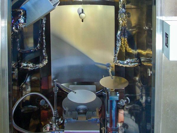
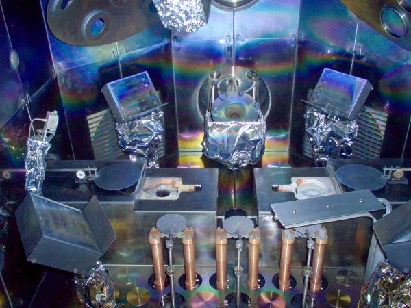
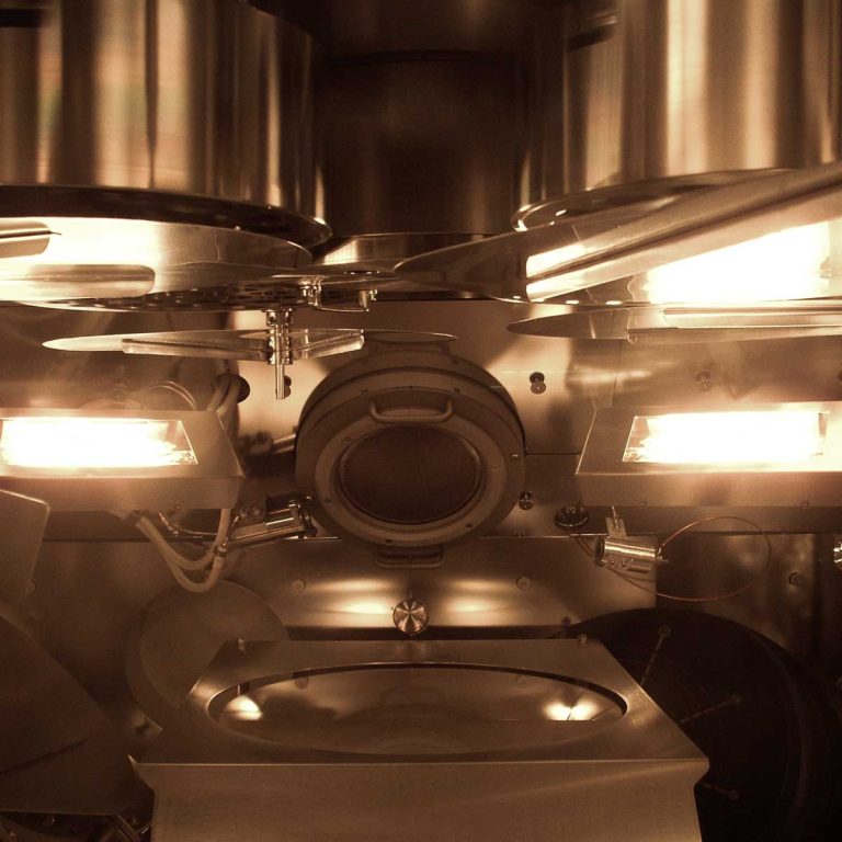
Ion Beam Assisted Deposition (IBAD) is a deposition technique that uses any deposition source to deposit the material onto a substrate which is bombarded by ions coming from an ion beam source. This process enables the deposition of metals, semiconductors, dielectrics, and ceramics. During IBAD process the material to be deposited vaporizes and then condenses onto the substrate surface. At the same time the thin film and the surface of the substrate are exposed to energetic ions emitted by the ion beam, causing the surface to undergo changes like densification, surface diffusion, and thin film nucleation. This technique can be used on more temperature-sensitive materials, such as plastics or polycarbonate lenses, since it can be performed at relatively low temperatures. The angle of the ion beam with the substrate is used to influence the roughness and texture of the film surface.
Applications
Ion Beam Assisted Deposition is a versatile thinfilm deposition technique widely utilized in the semiconductor, sensor industries to fabricate high-performance films with controlled properties
and top-quality optical coatings and in the medical industry for fabrication of metallic coatings
that are compatible with medical implants for biocompatibility or to create antimicrobial surfaces
- Consumer Electronics
- Automotive Industry
- Solar Energy
- Aerospace and defence
- Healthcare and medical devices
- Optics and photonics
- Surface engineering
Key features
- Low pressure processing (10-5 to 10-4 Torr range)
- Reduced porosity (higher density) in deposited films (low pressure means reduced included gas)
- High quality optical films with good stoichiometry, low optical absorption and smooth surfaces
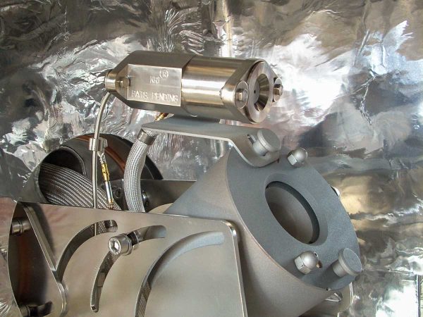
- An Assist Ion Beam is combined with a deposition source (Ion Beam, E–Beam, Sputtering depending on target material and layers)
- Substrate conditioning from –35 °C up to 800 °C
- Reactive gases (02 , N2 , H2 , etc) can be added for direct reaction during deposition process
- Optional automatic or manual load lock with optional pre-heating and/or plasma treatments
- Optional full optical thickness monitor for an unlimited number of layers by T% or R% wavelength scans on the coated substrates
Deposited materials
Metals, Oxides, Nitrides, Carbides, Semiconductors, Carbon Based Materials
Similar technologies

Ion Beam Assisted Deposition
the best choice for high end optical coatings