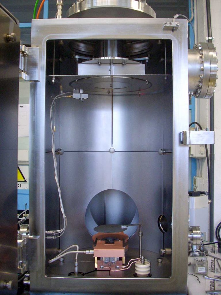
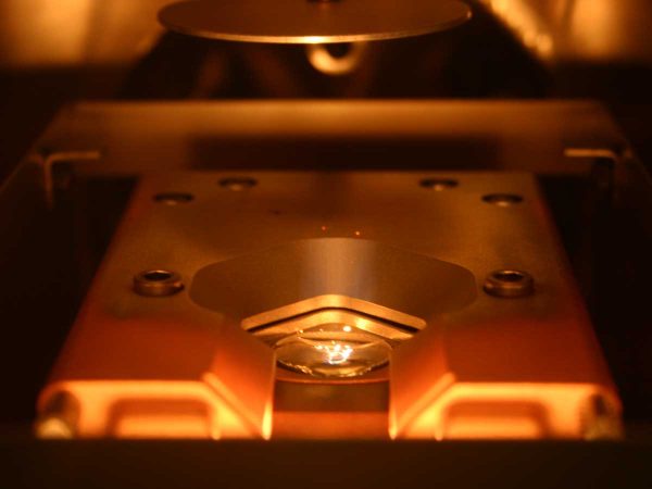
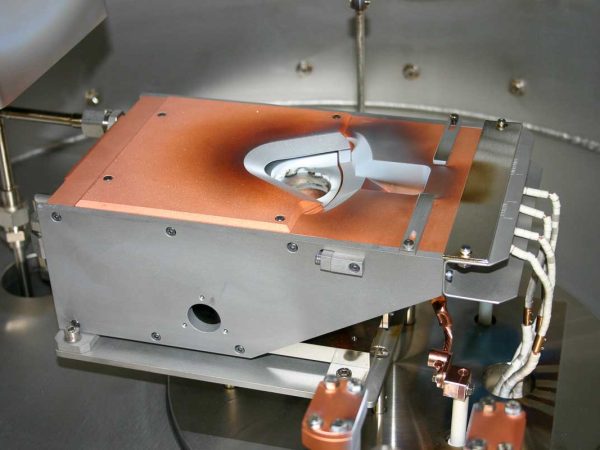
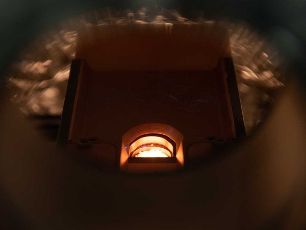
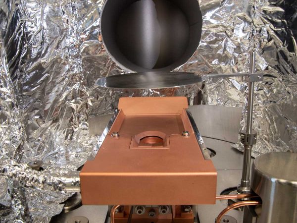
Electron Beam Evaporation (EBPVD) is a physical deposition technique used to create thin films on a substrate surface by evaporating a solid material placed in a crucible. The e-beam is generated through the thermionic emission process, where an electric current passes through a tungsten filament, causing the filament to heat up and emit electrons. High voltage is then applied between the filament and the hearth, allowing the liberated electrons to accelerate towards the crucible, while a magnetic field focuses them into a beam. The collimated electron beam hits the material in the crucible, allowing the evaporation process and the aggregation on the substrate surface. Compared to thermal PVD, EBPVD allows high evaporation temperature materials deposition as thin films. Deposition rates using electron beam processes can vary from 1 nm per minute to several μm per minute, depending on the required structural and morphological film control.
Applications
E-beam evaporation finds widespread use in various industries, like semiconductor, thin-film solar, aerospace, and cutting and tool industries, for producing wear-resistant and thermal barrier coatings. This technique is used also to produce dielectric, optical coatings, and Josephson junctions and in micro and nano-fabrication for lift-off processes.
Automotive Industry
Consumer Electronics
Aerospace and Defence
Healthcare and medical devices
Optics and Photonics
Energy storage
Key features
OHFC copper hearth crucible with up to 8 pockets of various sizes
HV or UHV configuration
Fully integrated quartz crystal controller for the automatic control of the thickness
Optional reactive gases, such as oxygen or nitrogen useful to reactively deposit non-metallic films
Optional automatic or manual load lock with optional pre-heating and/or plasma treatments
Optional ion beam source for bombarding the substrates during deposition (Ion Beam Assisted Deposition - IBAD)
Evaporation sources come in various sizes and configurations, single or multiple pockets