CVD Process


Plasma Enhanced CVD
PECVD
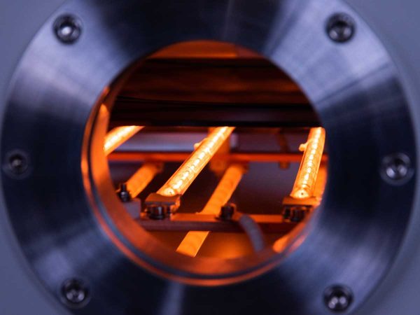
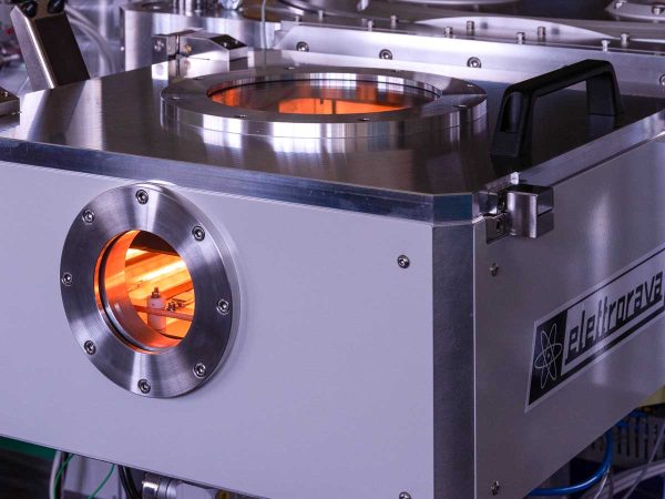
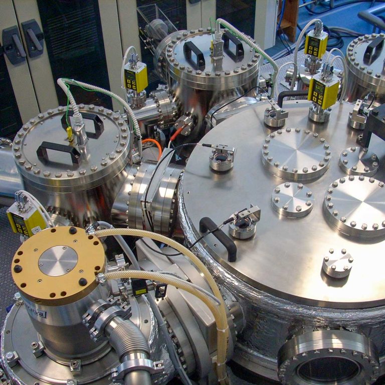
Plasma-enhanced chemical vapor deposition is a plasma-based deposition method used to deposit material on a substrate surface. PECVD is commonly used for depositing silicon oxide/nitride, hydrogenated amorphous and microcrystalline silicon and carbon, Diamond-like carbon (DLC), semiconductors and oxides. The process involves introducing a gas mixture into the vacuum chamber, where a plasma is generated. The process gases are ionized and decomposed into ions and radicals, which react with the substrate via chemical reactions, leading to the deposition of a thin film on the substrate. The plasma can be generated using different methods such as radio frequency (RF), alternating current (AC), or direct current (DC) discharge between two electrodes. PECVD offers a higher deposition rate while maintaining a lower temperature compared to thermal CVD
Applications
PECVD is used to produce high-quality semiconductor and dielectric films required for
various applications, like low and high-power semiconductor devices, photovoltaic solar
cells’ active layers, metal-insulator-metal (MIM) capacitors, laser diodes, sensors, detectors, LEDs, thin film transistors, and more.
- Consumer Electronics
- Automotive Industry
- Solar energy
- Aerospace and Defence
- Healthcare and medical devices
- Optics and Photonics
- Wear resistant coatings
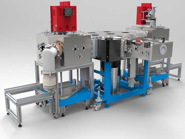
Key features
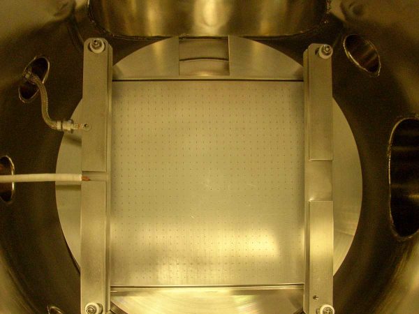
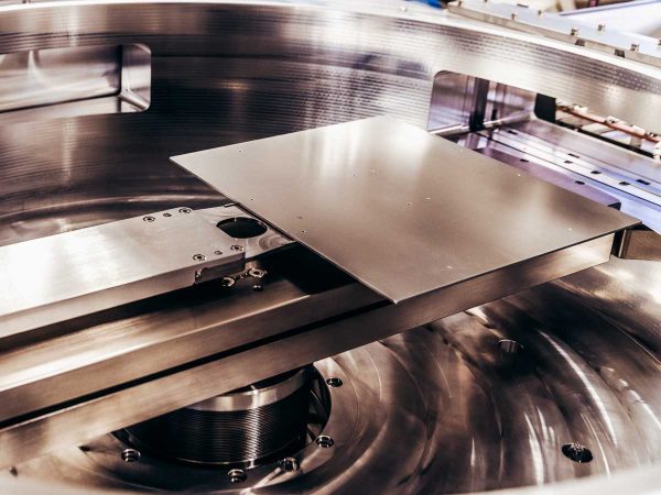
- RF showerhead electrode for uniform electric field and gas distribution
- Modular process gas manifold with mass flow controllers for up to 12 gases
- Optional vapor source controller for liquid Precursor (i.e. TEOS) with tank/cylinder in a closed cabinet for safe refill
- Automatic process pressure control
- Alternatively Hot Wire CVD
- In situ spectroscopic plasma monitoring
- Optional automatic or manual load lock (optional pre-heating and/ or plasma treatments)
- Optional wide range optical thickness monitor for the control of layer thickness
- Optional in situ spectroscopic ellipsometry for thickness measurement
Deposited materials
Metals, Oxides, Nitrides, Carbides, Semiconductors, Carbon Based Materials, Organics
Similar technologies

Plasma Enhanced CVD
the right choice for obtaining large area compound materials mixing gaseous and/or liquid precursors at any temperature